
唀匀䈀 ㌀⸀ 匀甀瀀攀爀猀瀀攀攀搀 倀䠀夀 吀攀猀琀 刀攀瀀漀爀琀ഀഀ
| Device Description | |
| Input File Path | Device 1 |
| Input Signal Type | Live signal |
| Reference Clock | SSC |
| De-emphasis Mode | -3.5 dB |
| Device | Device |
| Device ID: | Device 1 |
| Test Session Details | |
| Infiniium SW Version | 04.30.0004 |
| Infiniium Model Number | DSO91304A |
| Infiniium Serial Number | MY51500106 |
| Application SW Version | 1.42.9017 |
| Debug Mode Used | No |
| Compliance Limits (official) | USB 3.0 Specification version 1.0 |
| Probe (Channel 4) | |
| Last Test Date | |
| Margin Thresholds | |
| Warning | < ㈀ഀഀ % |
| Critical | < ഀഀ % |
| Pass | # Failed | # Trials | Test Name | Actual Value | Margin | Spec Range |
 | 0 | 1 | LFPS Peak-Peak Differential Output Voltage | 815.1 mV | 3.8 ─ഀഀ | 800.0 mV <= VALUE <= 1.2000 V |
| 0 | 1 | LFPS Period (tPeriod) | 39.8775 ns | 24.8 ─ഀഀ | 20.0000 ns <= VALUE <= 100.0000 ns |
| 0 | 1 | LFPS Burst Width (tBurst) | 1.0484 µs | 44.0 ─ഀഀ | 600.0 ns <= VALUE <= 1.4000 µs |
| 0 | 1 | LFPS Repeat Time Interval (tRepeat) | 10.0195 µs | 49.8 ─ഀഀ | 6.0000 µs <= VALUE <= 14.0000 µs |
| 0 | 1 | LFPS Rise Time | 242.0 ps | 94.0 ─ഀഀ | VALUE <= 4.0000 ns |
| 0 | 1 | LFPS Fall Time | 239.8 ps | 94.0 ─ഀഀ | VALUE <= 4.0000 ns |
| 0 | 1 | LFPS Duty cycle | 50.0172 % | 49.9 ─ഀഀ | 40.0000 % <= VALUE <= 60.0000 % |
| 0 | 1 | LFPS AC Common Mode Voltage | 45.0 mV | 55.0 ─ഀഀ | VALUE <= 100.0 mV |
| 0 | 1 | TSSC-Freq-Dev-Min | -5.074122 kppm | 6.3 ─ഀഀ | -5.300000 kppm <= VALUE <= -1.700000 kppm |
| 0 | 1 | TSSC-Freq-Dev-Max | 80.006 ppm | 36.7 ─ഀഀ | -300.000 ppm <= VALUE <= 300.000 ppm |
| 0 | 1 | SSC Modulation Rate | 30.576810 kHz | 19.2 ─ഀഀ | 30.000000 kHz <= VALUE <= 33.000000 kHz |
| 0 | 1 | SSC Slew Rate | 5.596 ms | 44.0 ─ഀഀ | VALUE <= 10.000 ms |
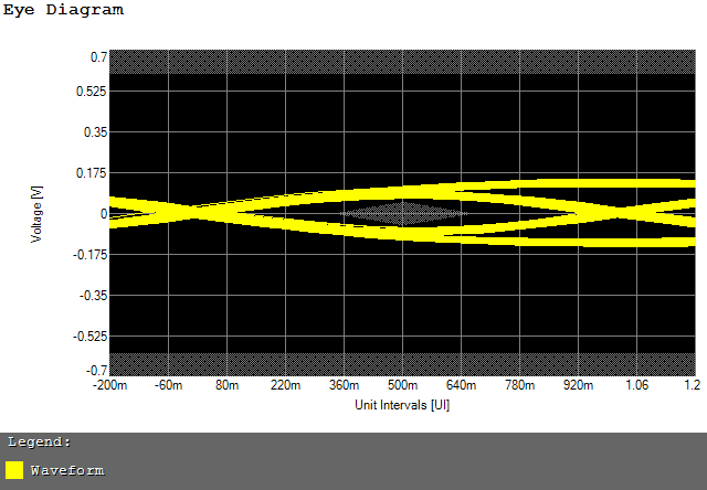
| 0 | 1 | Far End Random Jitter (CTLE ON) | 93 mUI | 59.6 ─ഀഀ | VALUE <= 230 mUI |
| 0 | 1 | Far End Maximum Deterministic Jitter (CTLE ON) | 137 mUI | 68.1 ─ഀഀ | VALUE <= 430 mUI |
| 0 | 1 | Far End Total Jitter at BER-12 (CTLE ON) | 231 mUI | 65.0 ─ഀഀ | VALUE <= 660 mUI |
| 0 | 1 | Far End Template Test (CTLE ON) | 0.000 | 100.0 ─ഀഀ | VALUE = 0.000 |
| 0 | 1 | Far End Differential Output Voltage (CTLE ON) | 122.4 mV | 2.0 ─ഀഀ | 100.0 mV <= VALUE <= 1.2000 V |
 LFPS Peak-Peak Differential Output Voltage
刀攀昀攀爀攀渀挀攀㨀ഀഀ
USB 3.0 Specification, Rev 1.0, Section 6.9, Table 6-20LFPS Period (tPeriod)
刀攀昀攀爀攀渀挀攀㨀ഀഀ
USB 3.0 Specification, Rev 1.0, Section 6.9, Table 6-20LFPS Burst Width (tBurst)
刀攀昀攀爀攀渀挀攀㨀ഀഀ
USB 3.0 Specification, Rev 1.0, Section 6.9, Table 6-21
LFPS Peak-Peak Differential Output Voltage
刀攀昀攀爀攀渀挀攀㨀ഀഀ
USB 3.0 Specification, Rev 1.0, Section 6.9, Table 6-20LFPS Period (tPeriod)
刀攀昀攀爀攀渀挀攀㨀ഀഀ
USB 3.0 Specification, Rev 1.0, Section 6.9, Table 6-20LFPS Burst Width (tBurst)
刀攀昀攀爀攀渀挀攀㨀ഀഀ
USB 3.0 Specification, Rev 1.0, Section 6.9, Table 6-21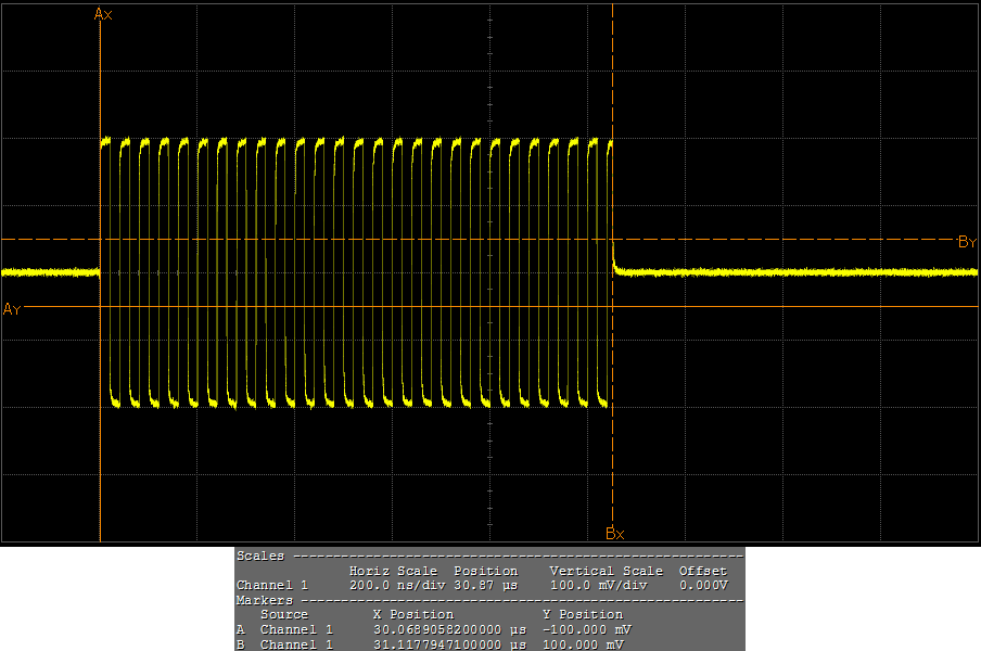 LFPS Repeat Time Interval (tRepeat)
刀攀昀攀爀攀渀挀攀㨀ഀഀ
USB 3.0 Specification, Rev 1.0, Section 6.9, Table 6-21
LFPS Repeat Time Interval (tRepeat)
刀攀昀攀爀攀渀挀攀㨀ഀഀ
USB 3.0 Specification, Rev 1.0, Section 6.9, Table 6-21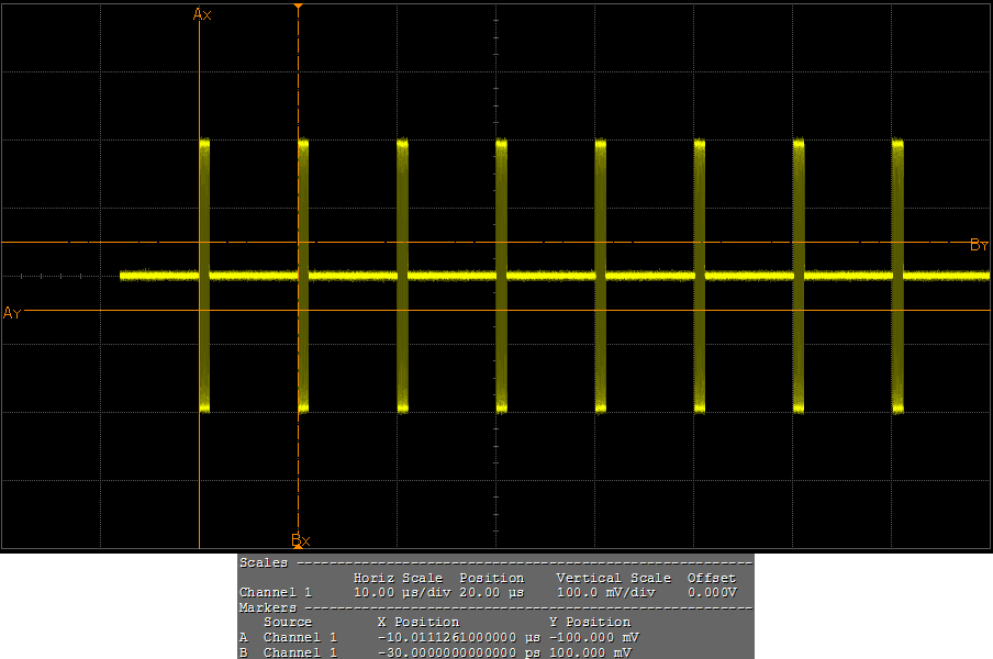 LFPS Rise Time
刀攀昀攀爀攀渀挀攀㨀ഀഀ
USB 3.0 Specification, Rev 1.0, Section 6.9, Table 6-20LFPS Fall Time
刀攀昀攀爀攀渀挀攀㨀ഀഀ
USB 3.0 Specification, Rev 1.0, Section 6.9, Table 6-20LFPS Duty cycle
刀攀昀攀爀攀渀挀攀㨀ഀഀ
USB 3.0 Specification, Rev 1.0, Section 6.9, Table 6-20LFPS AC Common Mode Voltage
刀攀昀攀爀攀渀挀攀㨀ഀഀ
USB 3.0 Specification, Rev 1.0, Section 6.9, Table 6-20TSSC-Freq-Dev-Min
刀攀昀攀爀攀渀挀攀㨀ഀഀ
USB 3.0 Specification, Rev 1.0, Section 6.5.3, Table 6-9
LFPS Rise Time
刀攀昀攀爀攀渀挀攀㨀ഀഀ
USB 3.0 Specification, Rev 1.0, Section 6.9, Table 6-20LFPS Fall Time
刀攀昀攀爀攀渀挀攀㨀ഀഀ
USB 3.0 Specification, Rev 1.0, Section 6.9, Table 6-20LFPS Duty cycle
刀攀昀攀爀攀渀挀攀㨀ഀഀ
USB 3.0 Specification, Rev 1.0, Section 6.9, Table 6-20LFPS AC Common Mode Voltage
刀攀昀攀爀攀渀挀攀㨀ഀഀ
USB 3.0 Specification, Rev 1.0, Section 6.9, Table 6-20TSSC-Freq-Dev-Min
刀攀昀攀爀攀渀挀攀㨀ഀഀ
USB 3.0 Specification, Rev 1.0, Section 6.5.3, Table 6-9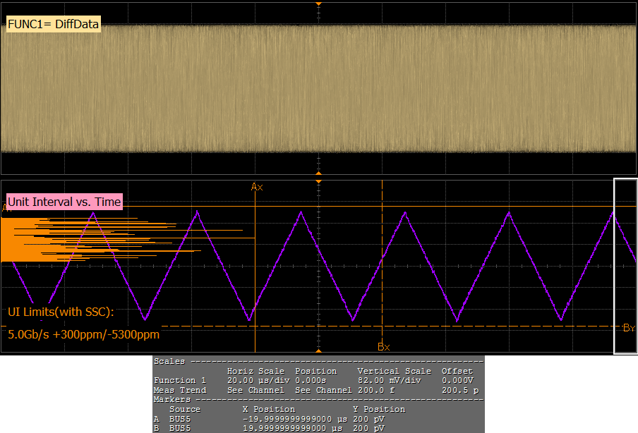 TSSC-Freq-Dev-Max
刀攀昀攀爀攀渀挀攀㨀ഀഀ
USB 3.0 Specification, Rev 1.0, Section 6.5.3, Table 6-9SSC Modulation Rate
刀攀昀攀爀攀渀挀攀㨀ഀഀ
USB 3.0 Specification, Rev 1.0, Section 6.5.3, Table 6-9SSC Slew Rate
刀攀昀攀爀攀渀挀攀㨀ഀഀ
USB 3.0 Specification, Rev 1.0, Section 6.7.1, Table 6-10
TSSC-Freq-Dev-Max
刀攀昀攀爀攀渀挀攀㨀ഀഀ
USB 3.0 Specification, Rev 1.0, Section 6.5.3, Table 6-9SSC Modulation Rate
刀攀昀攀爀攀渀挀攀㨀ഀഀ
USB 3.0 Specification, Rev 1.0, Section 6.5.3, Table 6-9SSC Slew Rate
刀攀昀攀爀攀渀挀攀㨀ഀഀ
USB 3.0 Specification, Rev 1.0, Section 6.7.1, Table 6-10 Far End Random Jitter (CTLE ON)
刀攀昀攀爀攀渀挀攀㨀ഀഀ
USB 3.0 Specification, Rev 1.0, Section 6.7.3, Table 6-12
Far End Random Jitter (CTLE ON)
刀攀昀攀爀攀渀挀攀㨀ഀഀ
USB 3.0 Specification, Rev 1.0, Section 6.7.3, Table 6-12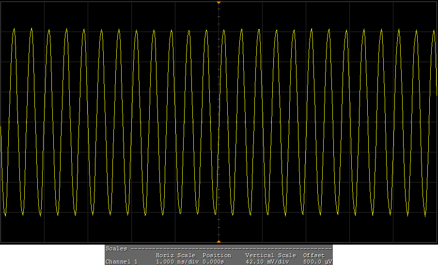 Far End Maximum Deterministic Jitter (CTLE ON)
刀攀昀攀爀攀渀挀攀㨀ഀഀ
USB 3.0 Specification, Rev 1.0, Section 6.7.3, Table 6-12Far End Total Jitter at BER-12 (CTLE ON)
刀攀昀攀爀攀渀挀攀㨀ഀഀ
USB 3.0 Specification, Rev 1.0, Section 6.7.3, Table 6-12Far End Template Test (CTLE ON)
刀攀昀攀爀攀渀挀攀㨀ഀഀ
USB 3.0 Specification, Rev 1.0, Section 6.7.3, Table 6-12
Far End Maximum Deterministic Jitter (CTLE ON)
刀攀昀攀爀攀渀挀攀㨀ഀഀ
USB 3.0 Specification, Rev 1.0, Section 6.7.3, Table 6-12Far End Total Jitter at BER-12 (CTLE ON)
刀攀昀攀爀攀渀挀攀㨀ഀഀ
USB 3.0 Specification, Rev 1.0, Section 6.7.3, Table 6-12Far End Template Test (CTLE ON)
刀攀昀攀爀攀渀挀攀㨀ഀഀ
USB 3.0 Specification, Rev 1.0, Section 6.7.3, Table 6-12
 Far End Differential Output Voltage (CTLE ON)
刀攀昀攀爀攀渀挀攀㨀ഀഀ
USB 3.0 Specification, Rev 1.0, Section 6.7.3, Table 6-12
Far End Differential Output Voltage (CTLE ON)
刀攀昀攀爀攀渀挀攀㨀ഀഀ
USB 3.0 Specification, Rev 1.0, Section 6.7.3, Table 6-12